Definition
A Zener diode is a type of diode that permits current to flow in the forward direction like a normal diode, but also in the reverse direction if the voltage is larger than the breakdown voltage known as Zener knee voltage or Zener voltage.
Basics

Current-voltage characteristic of a Zener diode with a breakdown
voltage of 17 volt. Notice the change of voltage scale between the
forward biased (positive) direction and the reverse biased (negative)
direction.
A Zener diode is a type of diode that permits current to flow in the forward direction like a normal diode, but also in the reverse direction if the voltage is larger than the breakdown voltage known as "Zener knee voltage" or "Zener voltage". Named for Clarence Zener, discoverer of this electrical property.
A conventional solid-state diode will not let significant current flow if it is reverse-biased
below its reverse breakdown voltage. By exceeding the reverse bias
breakdown voltage, a conventional diode is subject to high current flow
due to avalanche breakdown.
Unless this current is limited by external circuitry, the diode will be
permanently damaged. In case of large forward bias (current flow in the
direction of the arrow), the diode exhibits a voltage drop due to its
junction built-in voltage and internal resistance. The amount of the
voltage drop depends on the semiconductor material and the doping
concentrations.
A Zener diode exhibits almost the same properties, except the
device is specially designed so as to have a greatly reduced breakdown
voltage, the so-called Zener voltage. A Zener diode contains a heavily doped p-n junction allowing electrons to tunnel
from the valence band of the p-type material to the conduction band of
the n-type material. In the atomic model, this tunneling corresponds to
the ionization of covalent bonds. The Zener effect was discovered by physicist Clarence Melvin Zener.
A reverse-biased Zener diode will exhibit a controlled breakdown and
let the current flow to keep the voltage across the Zener diode at the
Zener voltage. For example, a diode with a Zener breakdown voltage of
3.2 V will exhibit a voltage drop of 3.2 V if reverse bias voltage
applied across it is more than its Zener voltage. However, the current
is not unlimited, so the Zener diode is typically used to generate a
reference voltage for an amplifier stage, or as a voltage stabilizer for low-current applications.
The breakdown voltage can be controlled quite accurately in the
doping process. Tolerances to within 0.05% are available though the
most widely used tolerances are 5% and 10%.
Another mechanism that produces a similar effect is the avalanche effect as in the avalanche diode.
The two types of diode are in fact constructed the same way and both
effects are present in diodes of this type. In silicon diodes up to
about 5.6 volts, the zener effect is the predominant effect and shows a marked negative temperature coefficient. Above 5.6 volts, the avalanche effect becomes predominant and exhibits a positive temperature coefficient.
In a 5.6 V diode, the two effects occur together and their
temperature coefficients neatly cancel each other out, thus the 5.6 V
diode is the component of choice in temperature critical applications.
Modern manufacturing techniques have produced devices with voltages
lower than 5.6 V with negligible temperature coefficients, but as
higher voltage devices are encountered, the temperature coefficient
rises dramatically. A 75 V diode has 10 times the coefficient of a 12 V
diode.
All such diodes, regardless of breakdown voltage, are usually marketed under the umbrella term of 'zener diode'.
Uses
Zener diodes are widely used to regulate the voltage across a
circuit. When connected in parallel with a variable voltage source so
that it is reverse biased, a zener diode conducts when the voltage
reaches the diode's reverse breakdown voltage. From that point it keeps
the voltage at that value.
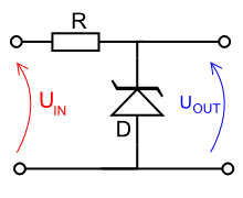
In the circuit shown, resistor R provides the voltage drop between UIN and UOUT. The value of R must satisfy two conditions:
- R must be small enough that the current through D keeps D in
reverse breakdown. The value of this current is given in the data sheet
for D. For example, the common BZX79C5V6 device, a 5.6 V 0.5 W zener diode, has a recommended reverse current of 5 mA. If insufficient current flows through D, then UOUT will be unregulated, and less than the nominal breakdown voltage (this differs to voltage regulator tubes where the output voltage will be higher then nominal and could rise as high as UIN). When calculating R, allowance must be made for any current flowing through the external load, not shown in this diagram, connected across UOUT.
- R must be large enough that the current through D does not destroy the device. If the current through D is ID, its breakdown voltage VB and its maximum power dissipation PMAX, then IDVB < PMAX.
A zener diode used in this way is known as a shunt voltage regulator (shunt, in this context, meaning connected in parallel, and voltage regulator being a class of circuit that produces a stable voltage across any load).
These devices are also encountered, typically in series with a
base/emitter junction, in transistor stages where selective choice of a
device centered around the avalanche/zener point can be used to
introduce compensating temperature co-efficient balancing of the
transistor PN junction. An example of this kind of use would be a DC error amplifier used in a stabilized power supply circuit feedback loop system.
Source: Wikipedia (All text is available under the terms of the GNU Free Documentation License and Creative Commons Attribution-ShareAlike License.)
|